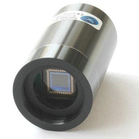
The professors at the University Of Rochester in New York, say they’ve managed to shrink cameras to the size of a shirt button and run “for years” on a single battery. The team has desinged a prototype chip that can digitize at each pixel, and are working on a second technology that will compress the image with far fewer computation that current compression techniques.
Here’s how the university’s press release describes the technology:
The first technology being developed integrates an oversampling “sigma-delta” analog-to-digital converter at each pixel location in a CMOS sensor. “CMOS” is a common semiconductor fabrication process used in most chips manufactured today. Previous attempts to do this on-pixel conversion have required far too many transistors, leaving too little area to collect light. The new designs use as few as three transistors per pixel, reserving nearly half of the pixel area for light collection. First tests on the chip show that at video rates of 30 frames per second it uses just 0.88 nanowatts per pixel—50 times less than the industry’s previous best. It also trounces conventional chips in dynamic range, which is the difference between the dimmest and brightest light it can record. Existing CMOS sensors can record light 1,000 times brighter than their dimmest detectable light, a dynamic range of 1:1,000, while the Rochester technology already demonstrates a dynamic range of 1:100,000.
Traditional image sensors use an array of light-sensitive diodes to detect incoming light, and transistors located at each photodiode to amplify and transmit the signal to an analog-to-digital converter located outside of the photodiode array. Other designs can convert the signal to digital at the pixel site, but require high precision transistors, which take up considerable chip space at each pixel and reduce the amount of surface area on the chip devoted to receiving light. The new design not only uses smaller transistors at each pixel, and thus can allow more light to be detected, but the transistors can be scaled down in size without diminishing the sensor performance as advances in semiconductor fabrication technologies allow the size of transistors to shrink. This means that much denser, higher-resolution chips can be developed without the prohibitive problems of the existing sensor designs. When transistors are reduced in size, they also become faster, allowing incoming light to be sampled more frequently and accurately.
What makes Bocko and Ignjatovic’s method work so elegantly is its feedback design. Traditional CMOS image detectors apply a voltage to charge up a photodiode, and incoming light triggers a release of some of that charge. An amplifying transistor then checks the remaining voltage on the diode, and the diode is recharged again. Bocko and Ignjatovic’s design also begins with a charged photodiode that discharges when light reaches it, but the discharge is then measured against a one/zero threshold and the resulting bit is delivered off the chip. If the result of a measurement is a one, then a packet of charge is fed back to the diode, effectively recharging it. The design also uses significantly less power than existing sensor designs, which is especially important in smaller devices like cell phones and digital cameras where battery size is restricted.
The second advance has taken many researchers by surprise. Called “Focal Plane Image Compression,” Bocko and Ignjatovic have figured out a way to arrange photodiodes on an imaging chip so that compressing the resulting image demands as little as 1 percent of the computing power usually needed.
Normally, the light-detecting diodes on a chip are arranged in a regular grid—say 1,000 pixels by 1,000 pixels. A picture is snapped and each diode records the light hitting it. A computer in the camera then runs complex computations to compress the image so that instead of taking up 10 hefty megabytes, it might only take up 100 kilobytes. The common picture type “JPEG,” used on the Web and on many cameras and phones, is an example of this. This compression, unfortunately, takes a tremendous amount of computing power, and hence battery power.
Ignjatovic and Bocko of the Department of Electrical and Computer Engineering, came up with a way to make the physical layout of the light-sensitive diodes simplify the computation. The normal way to perform compression includes a computation called the discrete cosine transform, which checks how much a segment of an image resembles a series of cosine waves. Both the image and the cosine waves are sampled at regular intervals and the transform requires that the image and cosine wave samples be multiplied together and added. Since the cosine wave samples can have a value anywhere between -1and 1, the computation requires multiplication by non-integers, which demands the bulk of the computing power.
But Ignjatovic and Bocko have laid out the pixels to lie at the peaks of cosine waves resulting in a non-uniformly distributed array, instead of an evenly spaced one. By using this trick, the amount of computation required to compress the image is slashed by nearly five-fold. Since each pixel is positioned exactly where each cosine wave has a peak where the cosine value is “one,” multiplying by one is unnecessary. With no multiplication and only a little addition, the processor uses less power.


